Miniature Marvels
Ever wonder what’s under the hood of these advanced electronic devices that have proliferated our life in so many ways? Beneath the surface is a complex system of components arranged in configurations that resemble scaled versions of modern cities. The foundation for these miniature marvels is the integrated circuit (IC).
An IC is a combination of two or more electronic elements that are combined or connect into a system contained in a single package. A first attempt at this idea occurred in Germany in the 1920’s with the Loewe 3NF vacuum tube which integrated three tubes into one. Vacuum tubes were used in the receiver of radios. The motivation behind this advancement was to reduce the tax burden levied on radios which was a function of the number of tubes in the radio.
The first hybrid IC was developed by Jack Kilby in the mid 1950’s at Texas Instruments (TI) utilizing germanium substrate. Integrated circuit transistor count has increased exponentially doubling every two years following Moore’s Law and has reached 2.6 trillion MOSFET transistor junctions. With the advancements in miniaturizing electronics a common challenge still remains, how do you connect these devices to the outside world?

Figure 1 Smart phone circuit board with integrated circuits
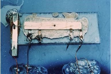
Figure 2 First hybrid IC developed by Jack Kilby in the mid 1950’s at Texas Instruments utilizing germanium substrate

Figure 3 Micron Technology’s NAND die using 20nm process can store 1 terabit of information
Bridging the Gap
Most often IC’s are required to interact with peripheral circuitry; so how do we connect these tiny devices to the outside world? You guessed it—a tiny wire!
This wire connection process is called wire bonding, which was developed by Bell Laboratories in the mid 1950’s. The initial process called thermocompression bonding involves heating the semiconductor surface to 200-300°C. Following this a wire is pressed down on the surface with a force of 5-10K lbs / in2 which produces a strong mechanical bond with excellent electrical properties. The machine that performs this task is called a thermocompression bonder, which became commercially available in the late 1950’s.
Ultrasonic bonding is an additional process that became available in the 1960’s and was derived from a welding technique developed in the 1950’s. Ultrasonic bonding involves rubbing two pieces of metal together until the surface impurities are removed by friction and atomic bonding is achieved. The final process for wire bonding is thermosonic bonding which is a combination of both thermocompression and ultrasonic bonding.
The primary advantages between these processes relate to the type of metals used and the bonding connection type utilized. Four bond wire material types are used, gold (Au), silver (Ag), copper (Cu) and aluminum (Al). There are two bond types, the wedge and the ball bond. Ultrasonic wiring bonding is almost exclusively used for Al wire with a wedge bond connection. Both thermocompression and thermosonic wire bonding can produce wedge or ball bond connections. Thermocompression is limited to Au bond wires while thermosonic can utilize Au or Cu. Thermosonic process comprises 90% of all wire boding, typically utilizing Au bond wires. Common reliability considerations are cratering or peeling of bond wire pads, wire bond fracturing, inconsistent tails (bond wire shorts), poor welding and improper positioning on the bond pad.

Figure 4 Wedge wire bonding IC die to lead packaging example utilizing Au bond wires
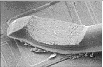
Figure 5 Electron microscope image of wedge wire bond connection
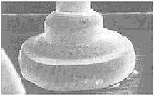
Figure 6 Electron microscope image of ball wire bond connection

Figure 7 Ultra fine pitch ball wire bonding produced by Kulicke and Soffa
Packaging Types
Packaging or enclosures for IC’s come in various forms depending on the application encapsulating several attributes, such as frequency of operation, environment, number of connections and cost. Frequency of operation is limited by the package die to lead inductance including the bond wire and package lead structure. Environmental considerations are temperature and moisture or humidity level. Cost is driven by the complexity of the die to package lead structure, the number of bond wire connections and packaging material.
There are several industry standard packages, BGA, DIP, QFN, SOIC, and TSSOP to name a few. Ball grid array (BGA) has high pin density, lower thermal resistance and low die to package lead inductance (high cost). Dual in-line package (DIP) on the other hand has, low pin density, high thermal resistance, high die to package lead inductance (low cost). The other packages fall within this range with varying tradeoffs.
Although packaging has steadily become more sophisticated adapting to higher pin count and operational frequencies, there are special case situations when it is necessary to interface directly with the circuitry. This is especial prevalent in microwave frequency and high-power applications.

Figure 8 Ball grid array (BGA) package depicting bond wire, die to substrate and lead to PWB interfaces

Figure 9 Dual in-line package (DIP)

Figure 10 Bare die application PWB mounted epoxy encapsulated
Packaging Influence
As the application frequency increases, so does the package influence on circuit performance. At frequencies in the 10’s of giga hertz the lead and bond wire parasitics can be substantial. The equivalent parasitic model for a bond wire includes shunt capacitance at the bond wire pad connection and series inductance attributed to the wire. The resistive component is a function of frequency and relates to the skin effect associated with the wire. The combination of these parasitics essentially form a frequency depended attenuator and lowpass filter that can limit the usable frequency of the device. This steadily becomes an issue with analog circuits that amplify, mix and manipulate signals above 1 GHz. This parasitic effect also limits the bandwidth available for a device.
To mitigate the influence of the bond wire and lead packaging as mentioned, the die can be directly mounted to the PWB or chassis thus eliminating the package leads. The number of bonding wires can also be tailored by the designer to optimize performance.
Thermal performance especially with high power microwave frequency designs is critical to the overall reliability, operating temperature range, output signal power limit and longevity. By bonding the die directly to one of the substrate copper layers or mounting structure, thermal resistance can be improved dramatically. This reduces the number of thermal contact layers and helps spread the thermal energy into the surrounding environment through conduction.
Typical substrates used for direct interaction with die for chip and wire applications is ceramic based (alumina) due to its low loss characteristics and hardness. It is essential to use a material with a high hardness to manage the wire bonding process.

Figure 11 Electrical parasitic model for bond wire connection between substrate and chip
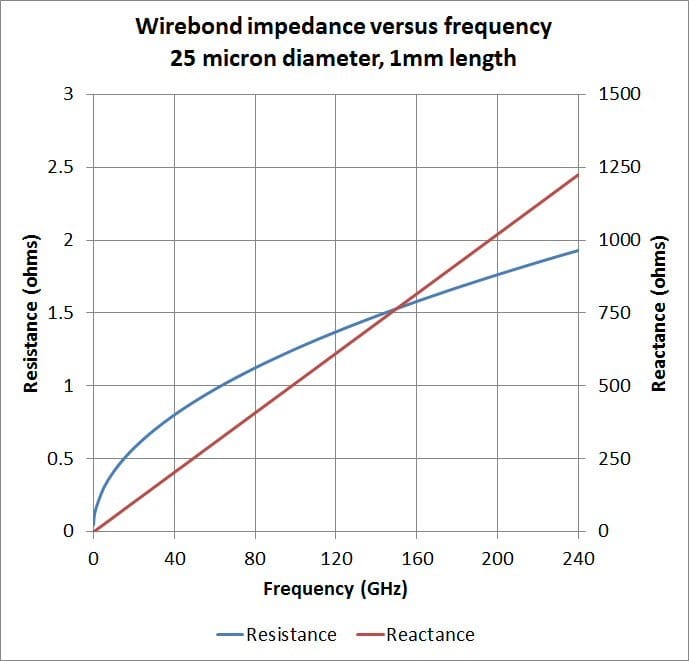
Figure 12 Inductance and resistance of a 25-micron diameter, 1mm length vs frequency bond wire model
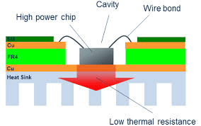
Figure 13 Cross section view of high-power chip mounted to the bottom copper layer of a print circuit as a method to improve thermal performance
Chip and Wire Applications
As mentioned, with an increase in frequency package influences can limit or hinder the use of devices especially in the microwave range. For cost and economies of scale, device manufacturers develop packages that cover a broad range of frequencies, unfortunately in this effort they are compromising or limiting the performance of these devices. Most often the die can operate at much higher frequencies but is limited by the available packaging. Fortunately, in most cases device manufacturers will sell the unpackaged (die form) version of their devices.
One of the many advantages of this approach is it lends itself to modularization. Each section of the design can be reused and interchangeably swapped out with other circuits based on specific need, even the carrier or chassis can be reused.
An approach that integrates microwave circuits into complete systems is the MMIC. One MMIC can accommodate several balanced amplifier circuits with mixers, control circuitry, etc; however, with less flexibility.
Additional considerations when choosing chip and wire as an option is the environment. Humidity and moisture can damage and influence devices; will most likely require hermetic sealing. The dies need to be protected from oxidation depending whether they are passivated.
As the market demand for features, bandwidth and integration increase so will the growth and need for chip and wire solutions. NuWaves is playing a critical role in this industry by providing cutting edge broadband, bidirectional power amplifiers and filtering systems and is well positioned to address this market.
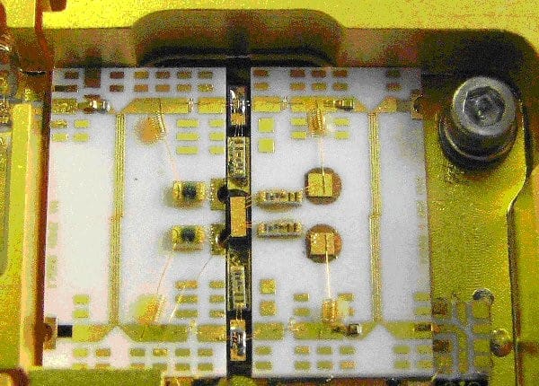
Figure 14 Balance amplifier occupying 0.3 square inches utilizing bare FET die devices and alumina substrate

Figure 15 Monolithic microwave integrated circuits (MMIC)
References
– Figure 1 – https://www.neowin.net/news/guide-to-smartphone-hardware-37-memory-and-storage/
– Figure 2 – https://en.wikipedia.org/wiki/Integrated_circuit#History/
– Figure 3 – https://investors.micron.com/news-releases/news-release-details/intel-micron-extend-nand-flash-technology-leadership
– Figure 4 – https://accelonix.co.uk/service-and-support/wirebonding-services
– Figure 5 / 6 – https://nepp.nasa.gov/index.cfm/20911
– Figure 7 – https://semiengineering.com/wirebond-technology-rolls-on/
– Figure 9 – https://zh.wikipedia.org/wiki/File:DIP_package_sideview.PNG
– Figure 10 – https://www.escomponents.com/baredie-101-what-is-bare-die
– Figure 11 – https://www.researchgate.net/figure/15-Bondwire-and-its-equivalent-circuit_fig60_336513333
– Figure 12 – https://www.microwaves101.com/encyclopedias/wirebond-impedance-and-attenuation
– Figure 13 / 14 – https://www.microwaves101.com/encyclopedias/chip-wire-construction


Comments are closed