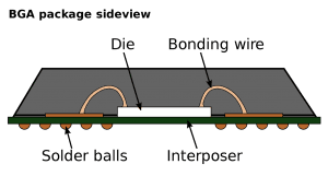
Ball grid array (BGA) is a method of surface-mount packaging used for integrated circuits (ICs), whereby the entire bottom surface of the IC is covered with an array of small solder balls to permanently mount devices such as microcontrollers, microprocessors, RAM devices, etc. to printed circuit boards. BGAs support a higher pin-count compared to the more traditional wire-bonded packaging to provide higher interconnection density for increased capability and/or smaller mounting footprint. BGAs also offer reduction in package thickness.

BGAs offer better electrical conductivity compared to other surface-mount packaging methods due to the shorter path distance between the die and the circuit board. BGAs offer less inductance to support lower signal degradation and higher frequency designs. BGA packaging has lower thermal resistance between the BGA package and the circuit board, which allows heat to flow more easily from the component to the PCB to provide better heat dissipation and help prevent overheating. BGAs also have improved current distribution which minimizes IR drops.
BGAs offer manufacturing advantages for OEMs as well. They allow for increased manufacturing yields due to overall improved soldering. The Assembly of BGAs onto circuit boards is more efficient and manageable than its lead counterparts because the solder needed for soldering the package onto the PCB comes from the solder balls itself. These solder balls also align themselves during mounting.
BGAs do have inherent disadvantages that should also be considered when choosing your surface-mount package. BGA packages are more prone to stress because of flexural stress from the circuit board, leading to potential reliability issues. Bending due to the difference in coefficient of thermal expansion between the PCB substrate and BGA can also cause solder balls to fracture as they cannot flex in the same way that longer leads can. Additionally, inspecting solder balls and solder joints for defects is incredibly difficult once the package is soldered down, and will usually require specialized equipment such as an x-ray machine.
BGAs can offer smaller design packages and higher performance out of their hardware. NuWaves has been investing in their BGA surface-mount packaging capabilities and has experience manufacturing products and hardware using BGA surface-mount packaging. NuWaves has significant experience with most common BGA footprints ranging from 100 through +1100 solder balls. Additionally, NuWaves has recently started a new project assembling a FPGA that utilize a +2300 BGA point footprint. This FPGA is the first of its kind and is being assembled as an eval-board for the customer.
Regardless of your products’ manufacturing requirements, NuWaves has the in-house manufacturing, production, and assembly capabilities to build-to-print with the most demanding build specifications and tolerances in mind, to provide you with the highest quality product.


